Will Silicon Photonics Transform Data Centers?
Silicon photonics is a technology that promises inexpensive, mass-produced optical components through photonics integration – it transfers data among computer chips by optical rays that carry more data in less time than electrical conductors. Since the first commercial product was introduced in 2005, the last decade has seen significant progress in technology and development.
A main application area for silicon photonics is cloud data centers, whose footprints continue to grow substantially to accommodate massive amounts of servers and switches. Starting in 2016, many hyperscale cloud content and service providers, such as Facebook and Microsoft, began deploying 100G Ethernet using singlemode optics-based infrastructure in their new data centers to support business growth.
100G Ethernet data center deployment has drawn much attention to silicon photonics; many of these singlemode transceiver modules are made with silicon photonics technology.
Let’s take a closer look at the applications, technology basics and market potential for silicon photonics.
Primary Applications
The first proof-of-concept experiment was conducted by Professor Richard Soref in 1985, but it took close to 20 years for the technology to advance from a core idea to a product (Kotura’s variable optical attenuator). The last decade has seen significant progress in product development.
Silicon photonics is also referred to as CMOS (complementary metal-oxide-semiconductor) photonics; these new types of photonic chips are produced with the same well-developed production infrastructure used for CMOS electronic chips. This ensures low costs, high yield and extremely small sizes to unleash a range of new optical devices for different applications:
- 100G/200G/400G mid-reach singlemode transceivers (500 m to 2 km) for intra-data-center interconnects, with modules such as PSM4/DR4 (parallel singlemode fibers)
- CWDM4/CLR4/FR4 (wavelength multiplexing over duplex fiber pair)
- 100G (or beyond) long-reach inter-data-center networks, also referred as data center interconnect (DCI), which connects data center clusters together using coherent optics (e.g. CFP2-ACO, CFP8-ACO) or direct modulation (<100 km)
- Large-scale data centers spread across a campus in a few buildings
- Data center buildings across metropolitan areas
- Optical transport networks and mobile front-haul networks
- Sensors for environmental monitoring in oil/gas industries and medical applications
CMOS Process
To better understand why silicon photonics is so appealing in certain industries, let’s take a look at the CMOS integrated circuit (IC) industry:
- Transistor: The semiconductor device that serves as the building block of modern IC and electronic devices, such as computers and cellphones. As predicted by the famous Moore’s Law, the number of transistors per square inch has doubled every 18 months for the past 50 years.
- CMOS: The core technology of IC mass-volume manufacturing processes for decades. Typically, hundreds or thousands of chips (millimeters in size) are processed in parallel on a single high-purity silicon wafer measuring 200 mm (8 inches) or 300 mm (12 inches) in diameter. Current-generation CMOS transistors made on wafers have feature sizes (half-pitch) as small as 14 nm (half the distance between identical features in an array), a fraction of the width of a human hair. (Feature size refers to a key dimension of a transistor.)
- CMOS Roadmap: The chip giants (e.g. Intel and TSMC) continue to shrink transistor size – the elemental switch used to make integrated circuits – because smaller nodes mean more transistors for computing/storage, less power consumption and lower cost per device. As transistor sizes now approach the atomic scale (fundamental physical limit), the International Technology Roadmap for Semiconductors (ITRS) predicts that 10 nm technology will be mainstream beginning in 2021.
Silicon photonics is attractive to the semiconductor industry: The investment and the developed expertise (i.e. CMOS processing, wafer-level testing and chip packaging) can be revamped for data transmission.
Historically, the optical components industry is much less mature in terms of component integration and volume shipment; the majority of photonics devices are assembled with discrete components and very high costs. Silicon photonics chip manufacturing can reuse the established CMOS IC process (200 mm and 300 mm wafer) with modifications to add photonics building blocks, such as light generation, modulation, waveguide, detection and passive components like multiplexers and splitters.
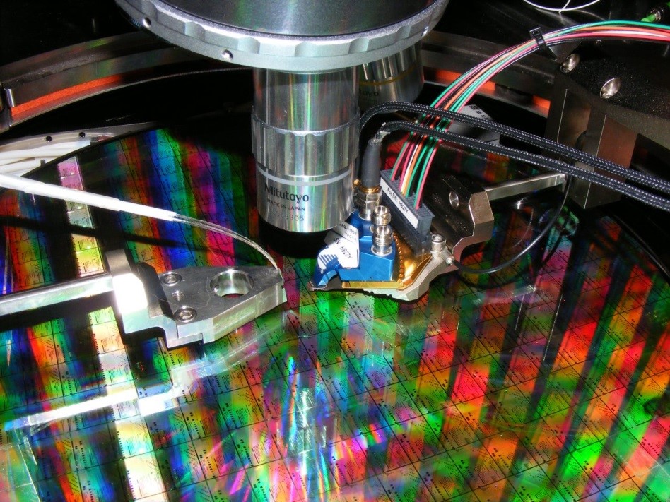
Automated wafer-level testing on silicon photonics wafer
Source: CEA-Leti
The IC chip achieves better performance by shrinking down the feature size. This is not equally true for the silicon photonics process; the minimum size of the waveguides is governed by the wavelength of the light source.
Typical light source wavelengths are within the range of 1310 nm, 1490 nm or 1550 nm; this is several orders of magnitude larger than the size of an electron. As a result, the larger-size features of the old CMOS processing nodes, such as 65 nm, 90 nm or 130 nm, are sufficient to make high-quality optical waveguides. These processes are currently well mastered and can operate at a much lower cost and higher yield as compared to the state-of-the-art 14 nm node CMOS IC process.
Technical Limitations
Mother Nature does not empower silicon with the best physical and chemical attributes for photonics integration. Historically, optical components are made using group III-V materials (on the periodic table), such as indium phosphide, gallium arsenide, lithium niobate and silica.
- As a group IV material on the periodic table, silicon is very stable. As a waveguide, it is subject to high material attenuation of ~2 db/cm, especially when compared to silica or group III-V material counterparts. Most silicon photonics devices are very small, so this is not a deal breaker; however, it sets design limitations for building complex structures, and overall performance is not as good as a group III-V platform, such as indium-phosphide.
- The typical silicon waveguide (refractive index = 3.5) size is less than 1 µm in diameter. Compared to singlemode fiber (germanium-doped silica, with refractive index = 1.47), which has a core size of 9 µm, the coupling on/off silicon waveguide to fiber requires special structures with extra coupling loss (e.g. inverted taper or grating couplers).
- Silicon does not lase (as a light source) when driven by electrons and cannot detect light. These two building blocks of an optical communications system – light generation and light detection – can be achieved by bonding extra material to the silicon substrate with additional process.
- Group III-V compounds (e.g. indium phosphide or gallium arsenide) can be bonded or monolithically developed on top of the silicon waveguide to generate light.
- Germanium is a common material added for light detection.
Challenges and Opportunities
Silicon photonics is still in its infancy. As suggested by LightCounting Research, it won’t be a disruptive technology in the next five years; product sales may reach $1 billion by 2020, accounting for 10% of the market.
As a matter of fact, its most important target application and market is data centers; it still competes against indium phosphide-based technology (InP) and VCSEL-based technology.
- In short-reach applications of up to a few hundred meters, VCSEL-based multimode optics are still the most cost-effective solution. Although the reach has shrunk to 100 m at 25G per lane and above, it can still satisfy most data center interconnect needs. Silicon photonics will have to become cheaper than multimode optics for the adoption of enterprise and Tier 2/Tier3 data centers.
- In middle-reach applications (0.5-2 km), silicon photonics transceivers are good contenders for hyperscale data centers, thanks to their low-cost structure; however, unlike in the IC industry, where common design tools and the CMOS process are used, each company currently has its own component design tool and component library. Each foundry has to change the manufacturing process for specific designs. Only a handful of companies can achieve the economy of scale with very high-volume production. For example, 100G-CWDM4 and 100G-PSM4 transceiver module shipments are not predominantly silicon photonics transceivers; the traditional InP-based technology can still compete with reasonable profit margin. It would be beneficial to have a common design platform for silicon photonics devices, but this cannot easily be achieved in the short term.
- For longer-reach applications, silicon photonics optics find it difficult to match the overall performance of InP-based optics due to technical limitations. It will take tight electronics and optics integration to achieve comparable performance.
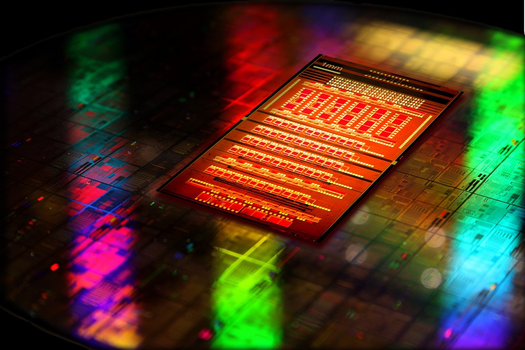
CMOS silicon photonics chip
Source: Here
Moving forward, on-board optics will help silicon photonics become even more pervasive, especially for high-performance computing platforms, also referred to as supercomputers. It will become an ideal technology that enables ultra-high density and high-speed I/O through the integration of photonics and electronics on a single platform. It is also a suitable technology that can enable large-scale Systems on Chip, which will emerge over the next few years.
If your organization is planning a next-generation Ethernet deployment and has unanswered questions, we can help! Belden data center experts can explain how silicon photonics may impact your future planning and budgeting, and help you decide if it’s worth exploring.
About the Author
![System.String[]](https://assets.belden.com/transform/d88d257f-c23d-4a61-b354-d49d9932ec65/qing-xu?io=transform:fill,width:300,height:300)
With 13 years of experience in optical communications and photonics device design, Qing Xu is a subject-matter expert in not only optical fiber technology, but also signal transmission, data center trends, fiber/copper connectivity and structured cabling. During his time with Belden, he closely monitored and participated in industry activities related to optical fiber communications systems, data center technology and trends.